Updated: 19 Jan 2010
Additions to bootstrap section


DESIGN WITH DISCRETE TRANSISTORS |
Updated: 19 Jan 2010 |
![]()
![]()
THE BASIC DISTORTION PERFORMANCE
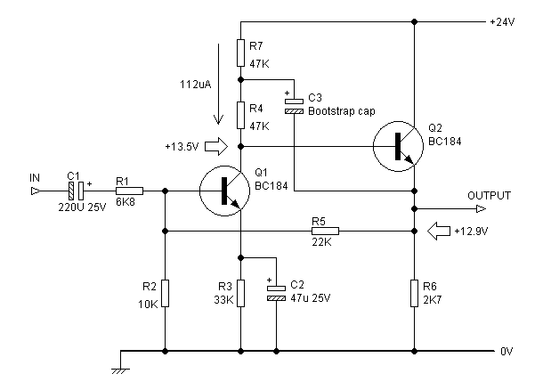 | Figure 1:Two-transistor shunt-feedback amplifier. The first stage Q1 has a bootstrapped collector load R4 to increase the open-loop gain; note the low collector current, a result of the high value of the collector resistors. The second stage is an emitter-follower which provides no voltage gain but buffers the high impedance at Q1 collector from the feedback network and external loads. The shunt feedback is via R5. |
As is usual with discrete configurations, the linearity is quite a strong function of the supply voltage, and in many cases the best way to improve the distortion performance is simply to raise this voltage. This obviously increases the power consumed by the configuration, but this is not normally a major issue.
Table 1
SUPPLY VOLTAGETHD 1 kHzIMPROVEMENT RATIO
+240.00435%1.00
+300.00324%0.74
+360.00262%0.60
+400.00228%0.52
+450.00201%0.46
+480.00188%0.43 |
The distortion drops quickly at first, as the supply voltage is increased, but the improvement is less at higher voltages. The input was 1 Vrms and the output 3.23 Vrms. These measurements were all taken with R6 at 2K7, as shown in Figure 1.
The noise output of the circuit in Figure 1 is -99.5 dBu. To work out the Equivalent Input Noise (EIN) we need to know the noise gain at which the circuit works. This is not simply (R5/R1)+1, which evaluates as +12.5 dB, as it would be for the eqivalent opamp circuit, because we must also allow for the presence of the biasing resistor R2. This raises the noise gain to +16.2 dBu. In the typical application for this kind of circuit, that of virtual-earth summing amp, there would have been many input resistances R1, and the presence of R2 would have made relatively little difference to the noise performance.
As briefly mentioned in SSAD Chapter Three, choosing the right size for a bootstrap capacitor is not quite as straightforward as it appears. It looks as if quite a small value could be used because of the high impedance of the Q1 collector load in Figure 1. C4 effectively sees only the 47K impedance of R8 to the supply rail, and the -3 dB frequency using 2u2 for bootstrapping is 1.54 Hz. However, as shown in Figure 2, this gives an enormous rise in LF distortion, reaching 0.02% at 10 Hz.
The reason for this steep rise in THD is that bootstrapping as a means of gain enhancement requires the bootstrapped point to accurately follow the output of the voltage stage, because even small deviations from unity mean that the increase in collector impedance, and hence gain, is seriously compromised. Note that there is no requirement for R4 and R8 to be the same value.
![]()
NOISE PERFORMANCE
Armed with the true noise gain, we can work out the EIN as -115.7 dBu, which is basically the noise performance of the first stage, as it implements all the voltage gain.
It has to be said that I have so far made no attempt to optimise the noise performance of the circuit shown here. Increasing the first-stage collector current would probably reduce the noise with the feedback values shown.
![]()
BOOTSTRAPPING ISSUES
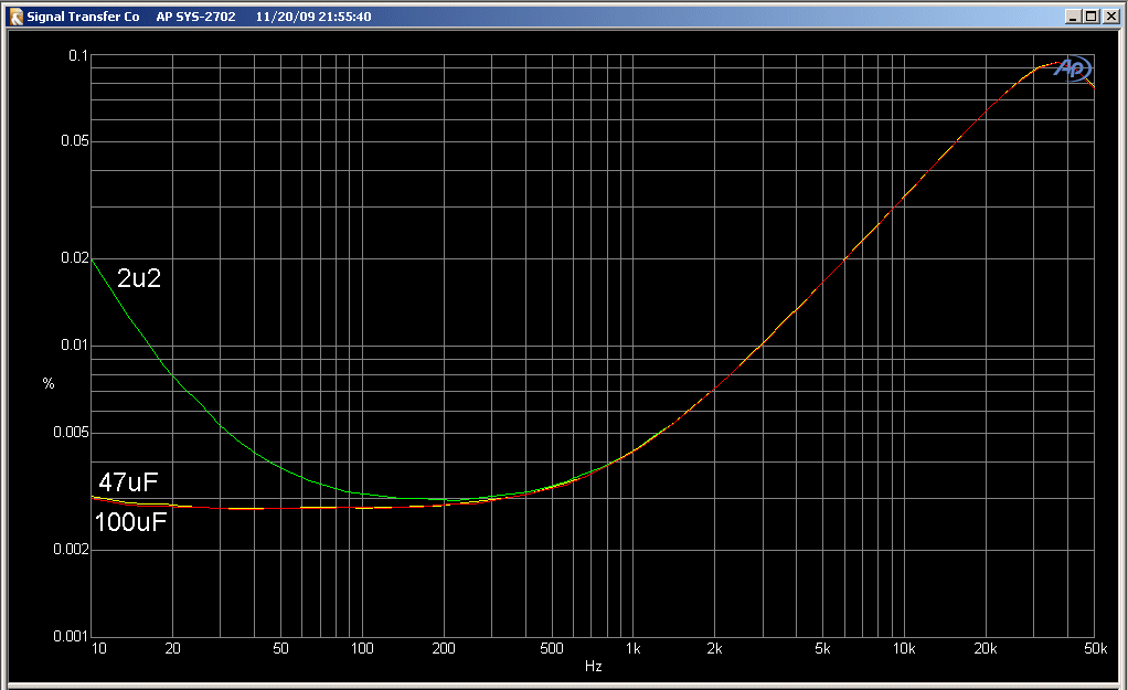 | |
Figure 2: The green trace shows the effect of using too small a bootstrap capacitor. (2u2) Output 3 Vrms, no external load. |
![]()
A convenient way to alter the curvature of the second stage is to vary the value of the emitter resistor R6 in Figure 1. The results of doing this are shown in Table 2.
The first row shows the standard results, as obtained from Figure 1 with R6 set to 2K7. Our first experiment is to raise its value to 3K3, but this is clearly a step in the wrong direction as THD increases from 0.00427% to 0.00466%. We therefore reduce R6 to 2K2, and get an immediate improvement to 0.00378%. Pressing on further, we reduce R6 to 2K0, and THD falls again, but this time by a smaller amount, giving 0.00360%. It looks as if further decreases will yield diminishing benefits, and we must also consider that we are increasing emitter-follower current, which may have serious consequences at higher supply voltages.
Table 2
SUPPLY VOLTAGER6 VALUETHD 1 kHzIMPROVEMENT RATIO
+242K70.00427%1.00
+243K30.00466%1.09
+242K20.00378%0.88
+242K00.00360%0.84
+302K00.00287%0.67
+362K00.00228%0.53
+402K00.00204%0.48
+452K00.00179%0.42
+482K00.00167%0.39 |
Looking at the first four rows of the table, it is clear we get a useful increase in distortion performance for no extra component cost at all.
As a general rule, any emitter-follower in a discrete transistor configuration can be inverted- in other words replaced by its complementary equivalent. This can be useful when attempting to cancel the distortion from different stages, as described in the previous section.
In Figure 3, the output emitter follower Q2 is now a PNP device.
![]()
INVERTING THE EMITTER-FOLLOWER
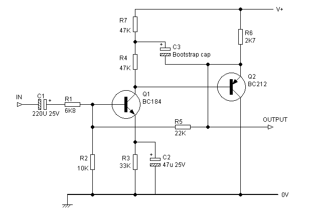 | Figure 3:Two-transistor shunt-feedback amplifier with the emitter-follower Q2 inverted. |
Unfortunately, in this case, we have royally messed up the existing distortion cancellation rather than improved it, as shown in Table 3. (The "Improvement ratio" is based on the original configuration; the top row of Table 2 is the reference) The distortion with a +24V rail is almost doubled.
Table 3
SUPPLY VOLTAGETHD 1 kHzIMPROVEMENT RATIO
+240.00850%1.99
+300.00711%1.66
+360.00589%1.38
+400.00521%1.22 |
We can again attempt to improve the linearity by modifying the value of the output emitter resistor R6, but it doesn't help much. The unimpressive results are seen in Table 4. The "Improvement ratio" is based on the original configuration; the top row of Table 2 is the reference.
Table 4
SUPPLY VOLTAGER6 VALUETHD 1 kHzIMPROVEMENT RATIO
+242K20.00882%2.06
+242K70.00850%1.99
+243K30.00806%1.89 |
Here we see that the distortion now varies with the value of R6 in the opposite way from Figure 1; reducing the emitter resistor increases distortion rather than reducing it. This is another indication that inverting the output emitter follower has altered the way that the curvatures of the two stages interact.
Clearly inverting the emitter-follower in this configuration is not a good idea.
There is, however, an interesting consequence of the inversion of the emitter-follower. We can now use what might be called DC-bootstrapping instead of bootstrapping with a capacitor. The collector load of Q1 is R4, and it is connected between the base and emitter of the output emitter-follower Q2, as shown in Figure 4.
![]()
DC BOOTSTRAPPING
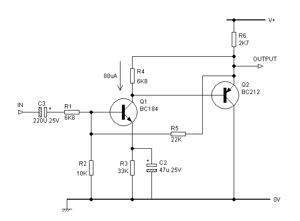 | Figure 4:Two-transistor shunt-feedback amplifier with emitter-follower Q2 inverted and DC-bootstrapping of the Q1 load R4. |
The distortion performance is summarised in Table 5. Once more, the "Improvement ratio" is based on the original configuration; the top row of Table 2 is the reference.
Table 5
SUPPLY VOLTAGER4 VALUER6 VALUETHD 1 kHzIMPROVEMENT RATIO
+246K82K70.00694%1.62
+246K83K30.00705%1.65
+246K82K20.00686%1.61
+244K72K70.014%3.28
+2410K2K70.015%3.51 |
This configuration has better linearity than the inverted emitter-follower with capacitive bootstrapping, but it is still markedly worse than the original version in Figure 1. As Table 5 shows, modifying R6 doesn't help much. We can try changing the value of the Q1 collector load R4, as it determines the Q1 collector current, and is likely to have an important effect on circuit operation, but as the last two rows of Table 5 demonstrate, sadly we find that either increasing or decreasing it from 6K8 makes things a lot worse.
We have however saved two components- the most important point being that an electrolytic capacitor has been eliminated, and these are the least reliable parts in the long-term, due to their tendency to dry out and drop in value. Configurations based on this kind of bootstrapping have been quite widely used in commercial equipment.
![]()

|